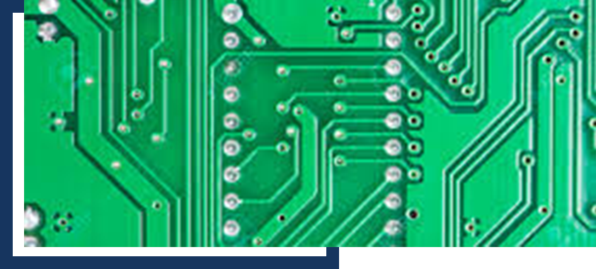
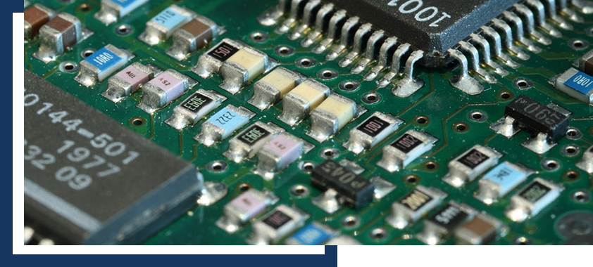
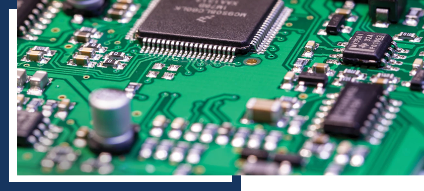
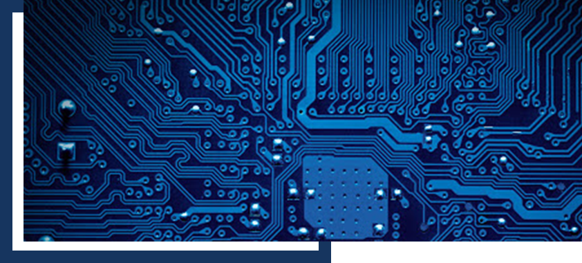
Tips on How to Properly Design/Manufacturing a Printed Circuit Board (PCB)

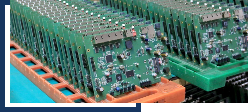
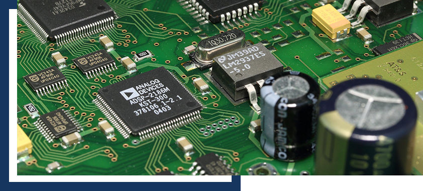
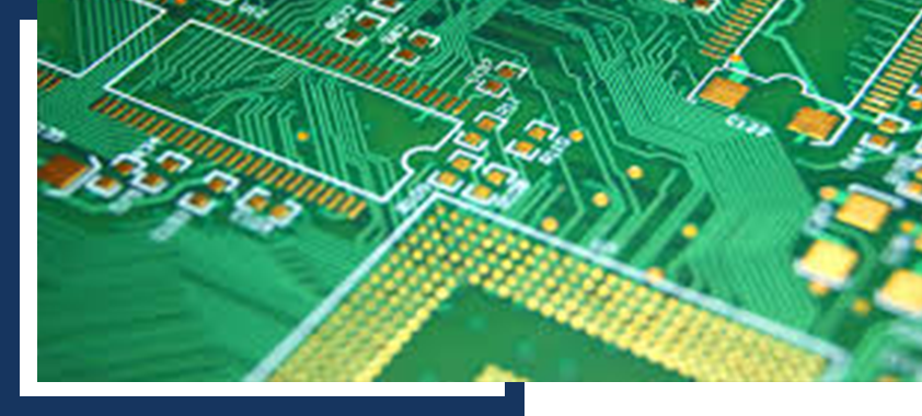
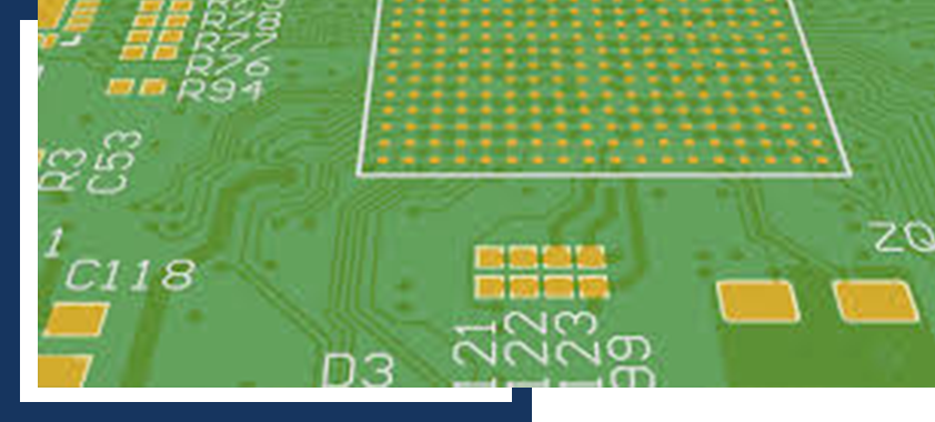
The Printed Circuit Board (PCB) is necessary for all the electronic devices that are used in both the residential and the commercial sector. It is used to design the electronic circuits. Besides it also provides mechanical supports to the component run by electricity. If you are an aspirant learning PCB designing and manufacturing, here are some tips as well as steps that the best electronics PCBA manufacturers follow.

About Us
About Us

Analysis and selection of components

The first step used by a professional Printed Circuit Board Manufacturer is to analyze deeply and select the appropriate components such as power supply and processor. Generating a blueprint for all the requirements is useful.

System front and design

Altium Designer, KiCad EDA, ORCAD, and Autodesk EAGLE are some easily available software used for PCB design by professional. Choosing the right application for you is important. The output of the designs is usually found in the form of a PCB Gerber file that encodes required information.

About Us
About Us

Photo tool initiation and print the inner layers

Running DFM before the circuit board fabrication is important to avoid any discrepancies. Photo film is required to be made to image the PCB. Cleanliness of the panel is important to avoid any short circuit. The film made before requiresplacing over the copper layer and aligning accordingly. Later the panel requires to be treated with UV rays again.

Etching out the unwanted copper

Later the panel needs to be washed again with a proper alkaline solution. Later a professional printed circuit board assembler prefers removing the copper layer and only leaves the required copper layer.

About Us
About Us

Layer up, bond and drilling

Professional PCB manufacture pastes the layer of PCB panel with aluminum press plate. For double and multi-layer PCB, copper foils require to be passed over the original layers. Finally, all the layers are pasted together to provide a final shape of PCB panels.

Copper deposition and platting

The next step requires covering the entire panels with a refreshed layer of copper. It helps the panels to bond and covers the nonconductive items opened up after being drilled. A chemical electrolysis set-up is very useful for plating. The entire drills holes need to be covered with more or less 25 microns of copper to secure a proper connection.

About Us
About Us

Other important tips

The best electronics PCBA manufacturer instructs to image outer layer and unwanted copper needs to be removed after that. The PCB needs to be plated with gold. The silk-screening or profiling comes under the printing of all critical information on the PCB such as id of the manufacturer, company name and number, the points of debugging etc. The best electronics PCBA manufacturers then prefer to run it through a proper electrical test. Then V-Cuts need to be made properly to permit the board to easily pop-out from the panel. At least it comes to final inspection that includes quality check.

These are some basic steps to follow to properly design the printed circuit board. For more information, you can contact an experienced printed circuit board supplier.