How to Get Printed Circuit Boards Manufactured and Assembled

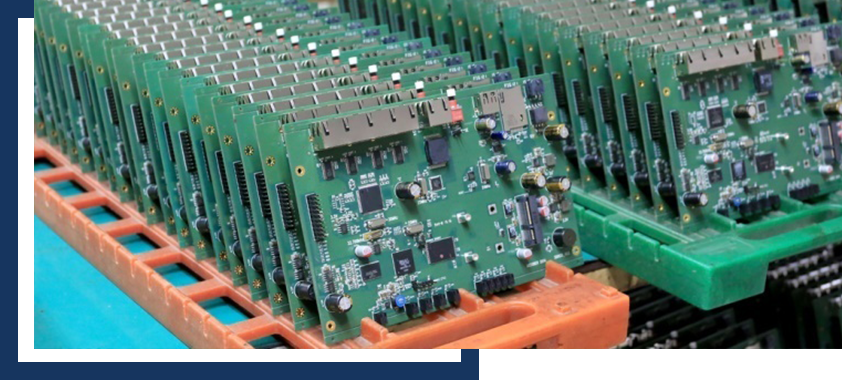
Printed circuit boards mainly manufactured and assembled to bring new electronic products in the market. We all know that electronic gadgets are an important part of our daily life. The smart phones, computers, and every electronic gadget are mainly included with printed circuit boards, this is also known as the heart of the electronic gadget, people also called it PCB.

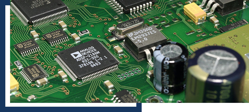
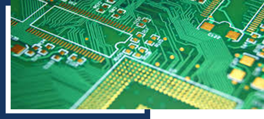
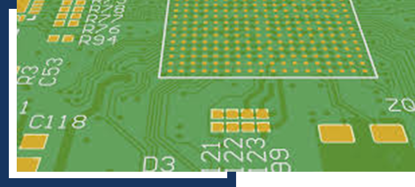
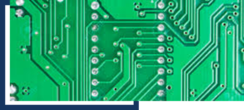
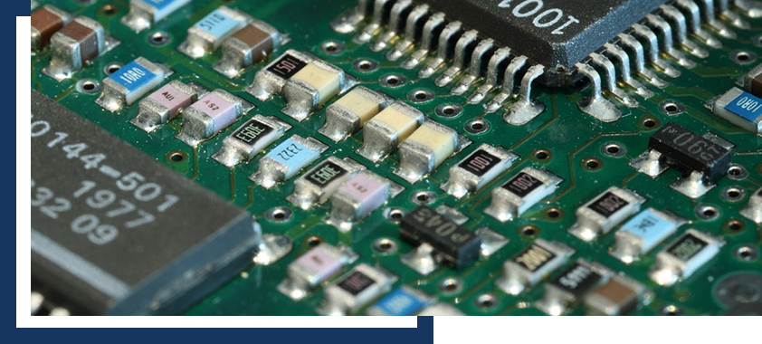
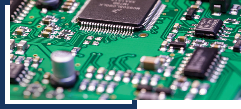
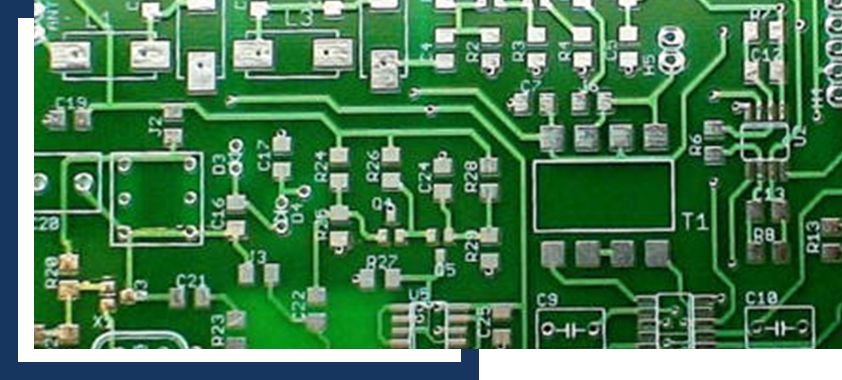
There are various electronic PCBA manufacturers and printed circuit board suppliers, who are delivering the best quality printed circuit boards. These are the small green chips covered in lines and copper parts, which you can find at the heart of every electric device and gadget. Without the printed circuit boards, electronic devices are not able to work. A PCB with components that are mounted on assembled PCB, the manufacturing process is known as PCB assembly.

About Us
About Us

Front process:

At the time of PCB manufacturing, most of the printed circuit board manufacturers first follow the PCB designs and prepare them for production. To begin this process each set design data and it assigned along with unique tools. It may happen customers re-order the exact same design and they want to make changes in the PCB, a new tool number become assigned. After completing the whole planning process the engineers become, ready to perform a new data review and they create a new PCB as per the requirement. These processes mainly included data clean up, drill and route data verification and edits, PCB edit process, penalization process, etc.

Photo plotting:

After completing the front and engineering process the next step is photo plotting. To make the printed circuit board thick many PCB manufacturers use bay area circuits. With the help of this special laser, direct imaging equipment images directly onto the dry film. It also helps to reduce the cost and it works in a more proper way.

About Us
About Us

Imaging and development:

To develop the printed circuit board Manufacturer, apply dry films to image the panel by using laser direct imaging. To develop the dry film all the printed circuit board areas exposed by the laser. The remaining film act as an etch barrier, which helps to prevent the conductive pattern.

Automated optical inspection process:

To manufacture and to assemble the printed board circuit automated optical inspection process becomes used to inspect the layers of a multi-layer PCB prior laminating the layers together. This process allows the manufacturer to inspect the defects in printed circuit boards. This inspection process is included with a decrease in the size of features, poor dry film resist adhesion, leaving unwanted copper, and creating reduced feature sizes and cuts.

About Us
About Us

OXIDE process:

OXIDE process mainly used at the time of manufacturing the printed board circuits, this is a chemical treatment to inner layers of the multiplayer before the PCB lamination. With the help of these processes, you can prevent separation between any of the layers of the base material. Not only that this process also helps to delamination between the laminate and conductive foil, while the manufacturing porches become done.

Lamination:

To make the Printed circuit board alternating layers of epoxy-infused fiberglass sheets becomes used; these are called prepreg core materials, which are laminated together. This process becomes happened at a high temperature only. At the time of making 4 layers or multilayer PCB to make it thicker, inner layer imaging becomes used, along with this process prepreg and outer copper layers become used.

Drilling:

At the time of the PCB drilling process, it needs to drill with wholes, which helps to attach the components. Besides that, it needs linking copper; layers together, or for the purpose of mounting the PCB in its housing.

About Us
About Us

Electro less copper deposition:

After completing the drilling process, a thin coating of copper deposited, with the help of hole walls and electro less plating process. With the help of thin conductive coating and copper fiberglass, the whole electro less copper deposition process becomes done.

The next step is dry film outer layer:

After the electro less copper deposition, the outer layer images need to prepare the panel; for electroplate. This process begins with the help of a laminator machine along with dry film and photo image able material.

Plate:

The next step in manufacturing the printed circuit boards is plating. Where the copper plates used as conductive patterns and on the walls of the printed circuit boards meet the design as per the requirements for the circuitry.

To make the printed circuit board various manufacturer and printed circuit board assembler follow these aforementioned processes. With the help of these processes, the everyday technology market is able to invent new electrical devices. We can say that the printed circuit boards are one of the best gifts of modern technology process.

About Us